| CPC H01L 21/44 (2013.01) [H01L 23/3114 (2013.01); H01L 23/485 (2013.01); H01L 23/552 (2013.01); H01L 24/12 (2013.01); H01L 27/0623 (2013.01); H01L 29/7834 (2013.01); H01L 21/561 (2013.01); H01L 23/3121 (2013.01); H01L 24/16 (2013.01); H01L 24/48 (2013.01); H01L 2224/16227 (2013.01); H01L 2224/48227 (2013.01); H01L 2224/97 (2013.01); H01L 2924/15313 (2013.01); H01L 2924/19041 (2013.01); H01L 2924/19042 (2013.01); H01L 2924/19043 (2013.01); H01L 2924/19105 (2013.01); H01L 2924/3025 (2013.01)] | 5 Claims |

|
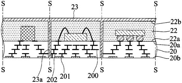
1. A method for fabricating an electronic package, comprising:
providing a substrate having a first side, a second side opposite to the first side, and a lateral side adjacent to the first side and the second side;
disposing an electronic component on the first side of the substrate, and electrically connecting the electronic component to the substrate;
forming on the substrate an encapsulant layer encapsulating the electronic component and having a first surface bonded to the first side of the substrate, a second surface opposite to the first surface, and a side surface adjacent to the first surface and the second surface; and
forming on the second surface of the encapsulant layer a shielding layer having an extending portion extending from a portion of an edge of the second surface of the encapsulant layer to the lateral side of the substrate along the side surface of the encapsulant layer, the extending portion being free from extending to the second side of the substrate, with a portion of the side surface of the encapsulant layer and a portion of the lateral side of the substrate exposed from the shielding layer, wherein the substrate has a grounding portion in contact with the shielding layer, the grounding portion communicates with the lateral side of the substrate and is in contact with the extending portion of the shielding layer, wherein the extending portion extends from a corner of the second surface of the encapsulant layer toward a corner of the second side of the substrate.
|