| CPC H01L 21/0274 (2013.01) [H01L 21/31144 (2013.01)] | 20 Claims |

|
1. A method of manufacturing a semiconductor device, comprising:
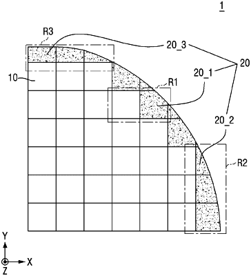
providing a substrate having, defined thereon, a die forming area and an edge die area, which includes a first cell area and a second cell area disposed between the first cell area and the die forming area;
sequentially forming a mold layer, a supporter layer, and a mask layer on the substrate;
forming an etch stopper film to cover a top surface of the first cell area, but not forming the etch stopper film on the second cell area;
forming a preliminary pattern layer on the etch stopper film and the mask layer;
forming first patterns, second patterns, and third patterns on the first cell area, the second cell area, and the die forming area, respectively, by exposing the preliminary pattern layer to extreme ultraviolet (EUV) light; and
forming hole patterns in the mold layer and the supporter layer in the die forming area and the second cell area by etching the mask layer using the etch stopper film, the second patterns, and the third patterns.
|
|
14. A method of manufacturing a semiconductor device, comprising:
providing a substrate having, defined thereon, a die forming area and an edge die area, which includes a first cell area and a second cell area disposed between the first cell area and the die forming area;
sequentially forming a mold layer, a supporter layer, and a mask layer on the substrate;
forming an etch stopper film to cover a top surface of the first cell area, but not forming the etch stopper film on the second cell area;
forming a preliminary pattern layer on the etch stopper film and the mask layer; and
forming first patterns, second patterns, and third patterns on the first cell area, the second cell area, and the die forming area, respectively, by exposing the preliminary pattern layer to light,
wherein
a top surface of the mask layer is disposed at the same height from the substrate, between the die forming area and the edge die area,
bottom surfaces of the first patterns, the second patterns, and the third patterns are sequentially higher than the substrate, and
at least some of the second patterns in the second cell area have a wedge shape that tapers down to a point toward the bottom thereof.
|
|
17. A method of manufacturing a semiconductor device, comprising:
providing a substrate having, defined thereon, a die forming area, an first edge die area which includes a first cell area and an second edge die area which includes a second cell area different from the first cell area;
sequentially forming a mold layer, a supporter layer, and a mask layer on the substrate;
forming an etch stopper film to cover top surfaces of the first and second cell areas, but not forming the etch stopper film on a dummy cell area between the first cell area and the die forming area and between the second cell area and the die forming area;
forming a preliminary pattern layer on the etch stopper film and the mask layer; and
forming first patterns, second patterns, and third patterns on the first and second cell areas, on the dummy cell area, and on the die forming area, respectively, by exposing the preliminary pattern layer to light,
wherein
at least some of the second patterns in the dummy cell area have a wedge shape that tapers down to a point toward the bottom thereof, and
a first width of the dummy cell area between the first cell area and the die forming area is different from a second width of the dummy cell area between the second cell area and the die forming area.
|