| CPC H01L 21/02529 (2013.01) [H01L 21/02032 (2013.01); H01L 21/02378 (2013.01); H01L 21/0243 (2013.01); H01L 21/02447 (2013.01); H01L 21/02502 (2013.01)] | 14 Claims |
|
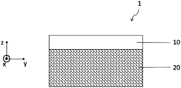
1. A method for producing a composite structure comprising a thin layer of monocrystalline silicon carbide on a carrier substrate made of polycrystalline silicon carbide, the method comprising:
providing an initial substrate comprising monocrystalline silicon carbide;
depositing an intermediate layer of polycrystalline silicon carbide at a temperature higher than 1000° C. on the initial substrate, a thickness of the intermediate layer being greater than or equal to 1.5 microns;
implanting light ionic species through the intermediate layer to form a buried brittle plane in the initial substrate, delimiting the thin layer between the buried brittle plane and the intermediate layer; and
depositing an additional layer of polycrystalline silicon carbide at a temperature higher than 1000° C. on the intermediate layer, the intermediate layer and the additional layer forming the carrier substrate, the initial substrate separating along the buried brittle plane during the deposition of the additional layer.
|