| CPC H01G 9/2009 (2013.01) [H10K 30/30 (2023.02); H10K 71/40 (2023.02); H10K 2102/00 (2023.02)] | 22 Claims |

|
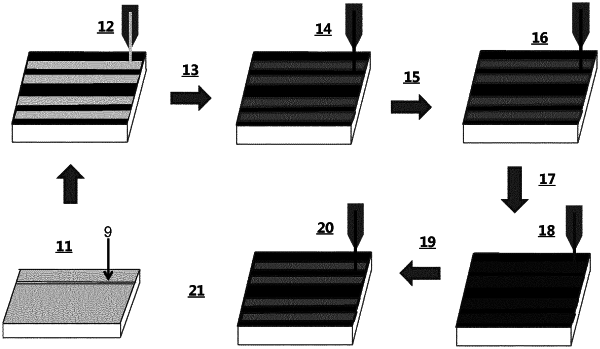
1. A method for producing layers of an electronic device comprising said layers, the method comprising:
depositing a first composition to provide a first film, wherein said first composition comprises the inorganic or carbon constituents of a first layer of said electronic device, or precursors of said inorganic constituents,
depositing a second composition to provide a second film, wherein said second composition comprises the inorganic or carbon constituents of a second layer of said optoelectronic device, or precursors of said inorganic constituents,
wherein said first and second compositions comprise, independently, at least one organic material,
wherein said second film is at least partially deposited onto the first film so as to at least partially superpose and/or overlap with said first film, and,
co-firing said two films by exposure to a temperature above 300° C., wherein, after depositing said first film, no firing above 300° C. is performed.
|