| CPC H01G 11/36 (2013.01) [H01G 11/56 (2013.01); H01M 10/0585 (2013.01); H01M 50/11 (2021.01); H05K 1/181 (2013.01); H05K 2201/10015 (2013.01); H05K 2201/10037 (2013.01)] | 31 Claims |
|
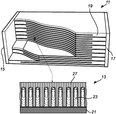
1. A discrete metal-insulator-metal (MIM) energy storage component, comprising:
a substrate having a first side and a second side opposite the first side;
a MIM-arrangement on the first side of the substrate, the MIM-arrangement comprising:
a first electrode layer deposited on the first side of the substrate;
a plurality of conductive nanostructures grown from said first electrode layer;
a conduction controlling material covering each conductive nanostructure in said plurality of conductive nanostructures and said first electrode layer left uncovered by said conductive nanostructures; and
a second electrode layer covering said conduction controlling material;
a first connecting structure for external electrical connection of said discrete MIM energy storage component;
a second connecting structure for external electrical connection of said discrete MIM energy storage component; and
an electrically insulating encapsulation material at least partly embedding said MIM-arrangement, in such a way that the electrically insulating encapsulation material at least partly forms an outer boundary surface of the discrete MIM energy storage component;
wherein the second side of the substrate at least partly forms the outer boundary surface of the discrete MIM energy storage component.
|