| CPC G11C 8/16 (2013.01) [G06F 30/392 (2020.01); G11C 11/418 (2013.01); G11C 11/419 (2013.01)] | 14 Claims |

|
1. A circuit comprising:
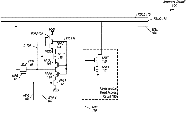
an array of memory bit cells configured to store data arranged as a plurality of rows and a plurality of columns, wherein:
a first portion of the plurality of rows are connected to a first read bit line of a given column of the plurality of columns and not connected to a second read bit line of the given column of the plurality of columns; and
a second portion of the plurality of rows are connected to the second read bit line and not connected to the first read bit line; and
circuitry configured to pre-charge one of the first read bit line and the second read bit line to a power supply reference level and pre-charge the other one of the first read bit line and second read bit line to a ground reference level;
wherein in response to receiving an indication of a first read operation targeting a row of the first portion comprising a first memory bit cell, the array of memory bit cells is configured to convey first data stored in the first memory bit cell to the first read bit line via a first asymmetrical read access circuit.
|