US 12,033,715 B2
Memory circuit arrangement for accurate and secure read
Vikas Rana, Noida (IN); and Arpit Vijayvergia, Bhopal (IN)
Assigned to STMicroelectronics International N.V., Geneva (CH)
Filed by STMicroelectronics International N.V., Geneva (CH)
Filed on Dec. 7, 2022, as Appl. No. 18/063,041.
Application 18/063,041 is a continuation of application No. 17/321,344, filed on May 14, 2021, granted, now 11,551,731.
Claims priority of provisional application 63/031,420, filed on May 28, 2020.
Prior Publication US 2023/0107851 A1, Apr. 6, 2023
Int. Cl. G11C 7/00 (2006.01); G11C 7/06 (2006.01); H03K 19/20 (2006.01)
CPC G11C 7/06 (2013.01) [H03K 19/20 (2013.01)] 22 Claims
OG exemplary drawing
 
1. A device, comprising:
a configurable memory array that includes:
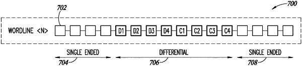
a plurality of rows of memory cells, the memory cells of at least one row including a plurality of user data memory cells, a plurality of test data memory cells, and a plurality of complementary test data memory cells, the plurality of complementary test data memory cells configured to store inverse data of the plurality of test data memory cells.