| CPC G11C 16/32 (2013.01) [G11C 16/0483 (2013.01); G11C 16/08 (2013.01); G11C 16/26 (2013.01); H10B 69/00 (2023.02)] | 18 Claims |
|
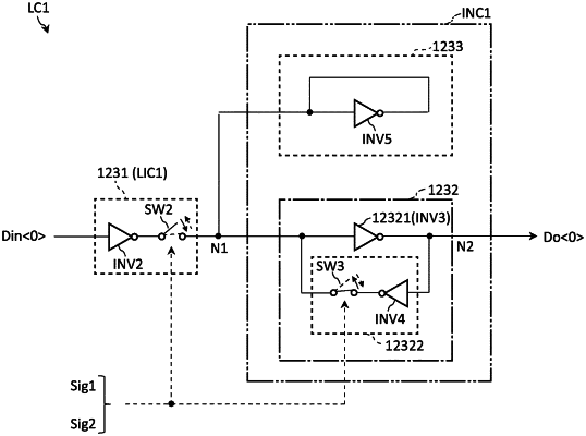
1. A semiconductor device comprising:
a first circuit configured to receive a first signal, and output a first voltage to a first node in accordance with a voltage of the first signal being at a first level and output a second voltage to the first node in accordance with the voltage of the first signal being at a second level, the first voltage being higher than the second voltage;
a second circuit coupled to the first node and configured to latch data based on a voltage of the first node; and
a third circuit coupled to the first node and configured to output a third voltage to the first node while the first circuit is outputting the first voltage to the first node and output a fourth voltage to the first node while the first circuit is outputting the second voltage to the first node, the third voltage being lower than the first voltage, and the fourth voltage being higher than the second voltage.
|