| CPC G11C 11/5678 (2013.01) [G11C 13/0004 (2013.01); G11C 13/0069 (2013.01); G11C 13/0097 (2013.01); G11C 2013/0073 (2013.01); G11C 2013/0078 (2013.01); G11C 2013/0092 (2013.01)] | 25 Claims |

|
1. A method for operating a memory array, comprising:
receiving a first command to store a first logic state in a memory cell comprising a chalcogenide material, wherein the memory cell is for storing three or more logic states;
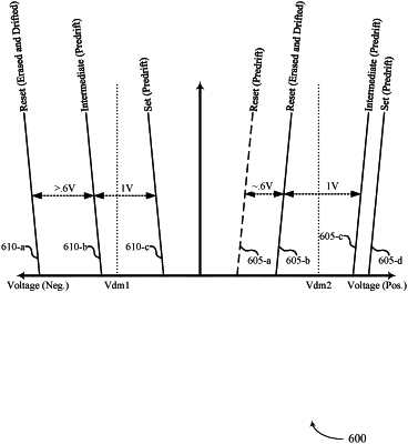
applying, as part of an erase operation, a first pulse with a first polarity to a plurality of memory cells to store a second logic state different from the first logic state in the plurality of memory cells, the plurality of memory cells comprising the memory cell, wherein applying the first pulse with the first polarity to the plurality of memory cells to store the second logic state comprises:
applying a first voltage to one or more word lines coupled with the plurality of memory cells; and
applying a second voltage to one or more digit lines coupled with the plurality of memory cells, wherein an absolute value of the second voltage is greater than an absolute value of the first voltage; and
applying, as part of a write operation, one or more second pulses with a second polarity to the memory cell to store the first logic state in the memory cell based at least in part on applying the first pulse to the plurality of memory cells, wherein applying the one or more second pulses with the second polarity to the memory cell to store the first logic state further comprises:
applying a third voltage to a word line coupled with the memory cell; and
applying one or more fourth voltages to a digit line coupled with the memory cell, wherein an absolute value of the one or more fourth voltages is greater than an absolute value of the third voltage.
|