| CPC G11C 11/5628 (2013.01) [G11C 11/5671 (2013.01); G11C 16/0483 (2013.01); G11C 16/08 (2013.01); G11C 16/10 (2013.01); G11C 16/26 (2013.01); G06F 12/0246 (2013.01)] | 20 Claims |

|
1. A memory system comprising:
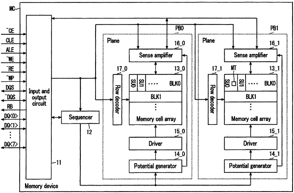
a semiconductor memory device including a first plurality of memory cells capable of storing n bits of data and a second plurality of memory cells capable of storing n bits of data (where n is a natural number equal to or greater than 2); and
a memory controller is configured to write first data and second data into the semiconductor memory device, wherein
the first plurality of memory cells and the second plurality of memory cells are capable of being read in parallel,
the memory controller is configured to write the first data into an i-th bit of the n bits of the first plurality of memory cells and the second data into a j-th bit of the n bits of the second plurality of memory cells, the j-th bit differing from the i-th bit,
a logical address of the first data is smaller than a logical address of the second data,
the logical address of the first data and the logical address of the second data are consecutive,
the memory controller is configured to transmit to the semiconductor memory device a first command to read the first data and a second command to read the second data,
the semiconductor memory device is configured to read the i-th bit of the first plurality of memory cells in response to the first command and read the j-th bit of the second plurality of memory cells in response to the second command, and
part of a read operation of the i-th hit of the first plurality of memory cells and part of a read operation of the j-th bit of the second plurality of memory cells are executed in parallel.
|