| CPC G11B 5/3146 (2013.01) [G11B 5/235 (2013.01); G11B 5/3133 (2013.01); G11B 5/314 (2013.01); G11B 5/37 (2013.01); H01F 10/329 (2013.01); H10B 61/00 (2023.02); H10N 50/85 (2023.02); H10N 52/00 (2023.02); H10N 52/80 (2023.02); C22C 19/07 (2013.01); G11B 2005/0024 (2013.01); G11B 5/39 (2013.01)] | 20 Claims |

|
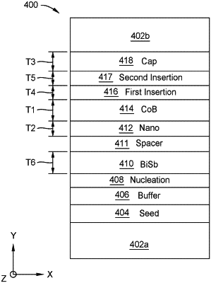
1. A spin-orbit torque (SOT) device, comprising:
a first electrode;
a seed layer disposed over the first electrode;
a cap layer spaced from the seed layer, wherein the cap layer is nonmagnetic;
a spin Hall layer;
a nano layer (NL) between the seed layer and the cap layer, wherein the NL is magnetic;
a cobalt-boron (CoB) layer between the seed layer and the cap layer, wherein the CoB layer is ferromagnetic and the CoB layer is substantially free from materials other than cobalt (Co) and boron (B), wherein there is spin orbital coupling between the CoB layer and the spin Hall layer; and
a second electrode disposed over the cap layer.
|