| CPC G09G 3/3266 (2013.01) [G09G 3/3233 (2013.01); G09G 2310/08 (2013.01); G09G 2330/028 (2013.01)] | 20 Claims |

|
1. A scan signal driver comprising:
a plurality of stages configured to be driven by dividing a first frame period into a display period and a sensing period, and to sequentially output scan signals at the display period,
wherein each of the plurality of stages comprises:
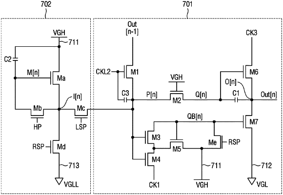
an output control circuit configured to control a Q node and a QB node; and
a memory control circuit configured to control an M node,
wherein the scan signal driver is configured to:
irregularly set a specific stage of the plurality of stages at the display period every frame;
control the specific stage to store a voltage, which is charged in the Q node, in the M node by using the memory control circuit based on the specific stage outputting a scan signal; and
control the specific stage to output a sensing signal by using the voltage stored in the M node at the sensing period subsequent to the display period, and
the memory control circuit included in each of the plurality of stages includes:
a first memory transistor configured to supply a high potential voltage to an I node based on a voltage level of the M node;
a second memory transistor configured to electrically connect the M node with the I node based on a holding signal input from outside;
a third memory transistor configured to electrically connect the output control circuit with the I node based on a line selection signal input from the outside; and
a fourth memory transistor configured to supply a second low potential voltage lower than a first low potential voltage to the I node based on a reset control signal input from the outside; and
a memory capacitor between the M node and a supply line of the high potential voltage.
|