| CPC G09G 3/3266 (2013.01) [H10K 59/121 (2023.02); H10K 59/131 (2023.02)] | 13 Claims |

|
1. A display device comprising:
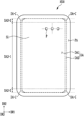
a substrate having a first display area and a second display area;
a first circuit disposed on the first display area of the substrate;
a first light emitting diode electrically connected to the first circuit and disposed in the first display area;
a second circuit disposed on the second display area of the substrate;
a second light emitting diode electrically connected to the second circuit and disposed in the second display area;
a first signal line crossing the first display area and electrically connected to a scan driver and connected to the first circuit disposed in a first row of the first display area and the second circuit disposed in a first row of the second display area, and
a second signal line connected to the first circuit disposed in a second row of the first display area and not connected to the second circuit disposed in a second row of the second display area,
wherein an area where light is emitted in the first display area is greater than an area where light is emitted in the second display area based on a same area.
|