| CPC G09G 3/3233 (2013.01) [G09G 3/2096 (2013.01); G09G 2300/0819 (2013.01); G09G 2300/0852 (2013.01); G09G 2310/0205 (2013.01); G09G 2310/0286 (2013.01); G09G 2310/08 (2013.01); G09G 2320/0209 (2013.01)] | 19 Claims |
|
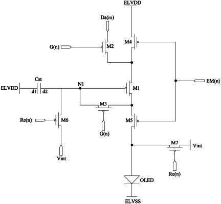
1. A drive method for a display panel, wherein the display panel comprises:
a plurality of pixels, configured to display a picture;
a plurality of pixel circuits, configured to control the plurality of pixels to emit light for display; and
a gate drive circuit arranged on a side of the plurality of pixel circuits and configured to output a gate scanning signal to the plurality of pixel circuits;
wherein the drive method comprises:
controlling, when the gate drive circuit scans the plurality of pixels line by line, a clock signal end to input a clock control signal to the gate drive circuit, to make the gate drive circuit to output the gate scanning signal, and controlling a data signal output by a data signal end to be written into a row of pixel circuits;
wherein an active level period of the clock control signal falls within an active level period of the data signal, and a start time of the active level period of the data signal is at least 1 μs-2 μs earlier than that of the active level period of the clock control signal;
wherein a duty ratio of the active level period of the data signal in a scanning period of a row of pixels is greater than 50%.
|