| CPC G09G 3/3233 (2013.01) [G09G 3/3266 (2013.01); G09G 3/3283 (2013.01); G09G 2300/0426 (2013.01); G09G 2300/0819 (2013.01); G09G 2300/0842 (2013.01); G09G 2300/0861 (2013.01); G09G 2310/061 (2013.01); G09G 2310/08 (2013.01); G09G 2320/043 (2013.01); G09G 2320/0626 (2013.01); G09G 2330/021 (2013.01)] | 15 Claims |

|
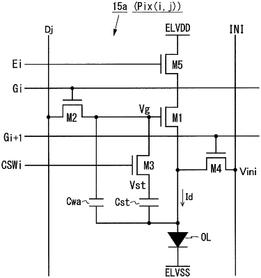
1. A display device comprising a plurality of data signal lines, a plurality of scanning signal lines intersecting the plurality of data signal lines, and a plurality of pixel circuits arranged along the plurality of data signal lines and the plurality of scanning signal lines, the display device further comprising:
a data signal line drive circuit configured to drive the plurality of data signal lines;
a scanning signal line drive circuit configured to selectively drive the plurality of scanning signal lines;
a plurality of capacitance selection signal lines each corresponding to one of the plurality of scanning signal lines; and
a capacitance selection control circuit configured to drive the plurality of capacitance selection signal lines,
wherein
each of the plurality of pixel circuits corresponds to one of the plurality of data signal lines and corresponds to one of the plurality of scanning signal lines,
each of the plurality of pixel circuits includes
a holding capacitor,
a display element having luminance controlled by a holding voltage held in the holding capacitor,
a writing control switching element having a writing control terminal connected to a corresponding one of the plurality of scanning signal lines,
an auxiliary writing capacitor having a capacitance value smaller than a capacitance value of the holding capacitor,
a capacitance selection switching element that has a capacitance control terminal connected to a corresponding one of the plurality of capacitance selection signal lines that is associated with the corresponding one of the plurality of scanning signal lines, the capacitance selection switching element being connected in series with the holding capacitor, and
an initialization circuit configured to discharge and initialize the holding capacitor before the capacitance selection switching element is turned on,
in each of the plurality of pixel circuits,
the auxiliary writing capacitor is connected in parallel with the holding capacitor and the capacitance selection switching element that are connected in series with each other, and
the auxiliary writing capacitor has a first terminal connected to a corresponding one of the plurality of data signal lines via the writing control switching element, and a second terminal connected directly or via a switching element to a fixed potential line,
when the corresponding one of the plurality of scanning signal lines is selected to turn on the writing control switching element, the auxiliary writing capacitor has a voltage of the corresponding one of the plurality of data signal lines applied thereto, so as to hold a writing voltage, and
when the corresponding one of the plurality of capacitance selection signal lines is activated to turn on the capacitance selection switching element, the holding voltage of the holding capacitor is determined on a basis of the writing voltage held in the auxiliary writing capacitor, wherein
the data signal line drive circuit is further configured to apply to each of the plurality of data signal lines a data voltage having an increased value depending on a ratio of the capacitance value of the holding capacitor to the capacitance value of the auxiliary writing capacitor, and
the capacitance selection control circuit is further configured to drive the plurality of capacitance selection signal lines such that after the voltage of the corresponding one of the plurality of data signal lines is written to the auxiliary writing capacitor while the holding capacitor is electrically disconnected from the corresponding one of the plurality of data signal lines, the auxiliary writing capacitor and the holding capacitor are connected in parallel with each other.
|