| CPC G09G 3/32 (2013.01) [G09G 2300/0819 (2013.01); G09G 2300/0852 (2013.01); G09G 2310/0202 (2013.01); G09G 2310/08 (2013.01); G09G 2320/0233 (2013.01); G09G 2330/021 (2013.01)] | 19 Claims |
|
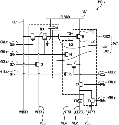
1. A display device, comprising
a display panel including a plurality of pixels, each including a pixel circuit and a light emitting element, a plurality of scan lines connected to the pixel circuit, an emission control line connected to the pixel circuit, and a data line connected to the pixel circuit,
wherein the pixel circuit includes:
a first capacitor connected to a first node and a second node opposite to the first node;
a first circuit portion including a first transistor and a second transistor, the first transistor being connected between the data line and the first node, and the second transistor being connected between the first transistor and the first node; and
a second circuit portion connected to the second node and the light emitting element,
wherein, before the light emitting element emits light, a reference voltage is provided to a third node between the first transistor and the second transistor,
wherein the first circuit portion further includes a third transistor connected between the third node and a reference voltage line to which the reference voltage is provided,
wherein the second circuit portion includes a fourth transistor connected between the second node and a first initialization voltage line to which a first initialization voltage is applied, and
wherein the second transistor and the fourth transistor are controlled by a same scan signal.
|