| CPC G09G 3/32 (2013.01) [G09G 2310/0267 (2013.01); G09G 2310/0275 (2013.01); G09G 2310/08 (2013.01)] | 30 Claims |

|
1. A display device comprising:
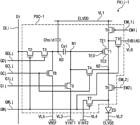
a pixel electrically connected to a data line, a write scan line, an initialization scan line, a compensation scan line, a transmission control line, and an emission control line and including a pixel circuit and a display element;
a first driving circuit configured to provide a write scan signal to the write scan line; and
a second driving circuit configured to:
receive a plurality of clock signals, each of which has a time duration of one unit horizontal period, and
provide an initialization scan signal, a compensation scan signal, a transmission control signal, and an emission control signal to the initialization scan line, the compensation scan line, the transmission control line, and the emission control line, respectively,
wherein each of the initialization scan signal and the compensation scan signal has an activation interval of two unit horizontal periods or more,
wherein the pixel circuit includes:
a first transistor including a gate electrode connected to a first node, a first electrode, and a second electrode connected to a second node;
a second transistor connected to the data line, an operation of the second transistor being controlled by the write scan signal provided to the write scan line; and
a third transistor connected between the second transistor and a third node, an operation of the third transistor being controlled by the transmission control signal provided to the transmission control line and different from the write scan signal.
|