| CPC G09G 3/2092 (2013.01) [G09G 2310/0297 (2013.01)] | 20 Claims |

|
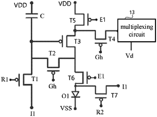
1. A multiplexing driving method for a display module, wherein the display module comprises a source driver, a gate driving circuit, a multiplexing circuit and a pixel circuit, pixel circuits in a same row are electrically connected to a same gate line, and pixel circuits in a same column are electrically connected to a same data line; the multiplexing circuit comprises at least one multiplexing sub-circuit comprising a plurality of multiplexing switches, a control end of each multiplexing switch in a same multiplexing sub-circuit is electrically connected to a multiplexing control end, a first end of the multiplexing switch is electrically connected to the source driver, a second end of the multiplexing switch is electrically connected to a corresponding data line, and a driving period comprises an initial time period, a first charging time period and a second charging time period arranged one after another; wherein, in the multiplexing sub-circuit, at least one multiplexing switch serves as a pre-charging multiplexing switch, and the multiplexing control end electrically connected to a control end of the pre-charging multiplexing switch is a pre-charging multiplexing control end; in the multiplexing sub-circuit, the multiplexing switches other than the at least one pre-charging multiplexing switch are non-pre-charging multiplexing switches, and the multiplexing control end electrically connected to a control end of each non-pre-charging multiplexing switch is a non-pre-charging multiplexing control end; the data line electrically connected to the pre-charging multiplexing switch is a pre-charging data line, and the data line electrically connected to each non-pre-charging multiplexing switch is a non-pre-charging data line;
wherein the multiplexing driving method comprises:
within the initial time period, applying an on control signal to the pre-charging multiplexing control end to turn on the pre-charging multiplexing switch, and applying, by the source driver, an initial voltage to the pre-charging multiplexing switch to write the initial voltage into the corresponding pre-charging data line via the turned-on pre-charging multiplexing switch, and applying an off control signal to the non-pre-charging multiplexing control end to turn off the non-pre-charging multiplexing switches;
within the first charging time period, applying an on control signal to different non-pre-charging multiplexing control ends in a time-division manner to turn on the different non-pre-charging multiplexing switches in the time-division manner; and applying, by the source driver, a corresponding grey-scale voltage to the non-pre-charging multiplexing switches to write the corresponding grey-scale voltage into corresponding non-pre-charging data lines in a time-division manner via the turned-on non-pre-charging multiplexing switches, and applying an off control signal to the pre-charging multiplexing control end to turn off the pre-charging multiplexing switches; and
within the second charging time period, controlling, by the gate driving circuit, a corresponding gate line to be turned on, to write the corresponding grey-scale voltage into the pixel circuits in a row corresponding to the gate line and electrically connected to the corresponding non-pre-charging data lines respectively; applying an on control signal to different pre-charging multiplexing control ends in a time-division manner to turn on the different pre-charging multiplexing switches in the time-division manner; applying an off control signal to the non-pre-charging multiplexing control end to turn off the non-pre-charging multiplexing switches; applying, by the source driver, a corresponding grey-scale voltage to the pre-charging multiplexing switches to write the corresponding grey-scale voltage to the pixel circuits in a row corresponding to the gate line and electrically connected to the corresponding pre-charging data lines respectively in a time-division manner via the turned-on pre-charging multiplexing switches; wherein each corresponding pre-charging data line is electrically connected to the turned-on pre-charging multiplexing switch.
|