| CPC G09G 3/20 (2013.01) [G11C 19/28 (2013.01); G09G 3/2092 (2013.01); G09G 3/3674 (2013.01); G09G 3/3677 (2013.01); G09G 2310/0202 (2013.01); G09G 2310/0267 (2013.01); G09G 2310/0286 (2013.01); G09G 2310/061 (2013.01); G09G 2310/08 (2013.01); G09G 2354/00 (2013.01)] | 20 Claims |

|
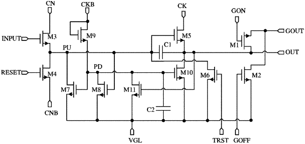
1. A shift register, comprising: a first output sub-circuit, a second output sub-circuit and a transfer sub-circuit, wherein the shift register comprises a signal output terminal and a line output terminal, the signal output terminal being connected with the first output sub-circuit and the second output sub-circuit, and the line output terminal being connected with the second sub-circuit and the transfer sub-circuit; wherein the line output terminal is connected with a pixel line, and the signal output terminal is not connected with the pixel line, only transfer and reset of shift register is performed;
the first output sub-circuit is configured to provide a signal of a first power supply terminal or a second power supply terminal to a pull-up node under control of a signal input terminal or a reset terminal, and output a signal of a first clock signal terminal to the signal output terminal according to a level of the pull-up node; transmit a signal of a second clock signal terminal to a pull-down node under control of the second clock signal terminal, and pull down a level of the signal output terminal according to a level of the pull-down node;
wherein the shift register is adapted to a visuosensory area with a plurality of scanning lines and a non-visuosensory area with a plurality of scanning lines; the second output sub-circuit is configured to output a signal of the signal output terminal to the line output terminal under control of a line-ON enable signal at a scanning output stage of the visuosensory area and a scanning output stage of the non-visuosensory area; and
the transfer sub-circuit is configured to pull down a level of the line output terminal under control of a line-OFF enable signal at a scanning transfer stage of the visuosensory area and a scanning transfer stage of the non-visuosensory area;
wherein the second output sub-circuit comprises a first transistor, a control electrode of the first transistor being connected with the line-ON enable terminal, a first electrode of the first transistor being connected with the signal output terminal, and a second electrode of the first transistor being connected with the line output terminal; and
wherein the transfer sub-circuit comprises a second transistor, a control electrode of the second transistor being connected with the line-OFF enable terminal, a first electrode of the second transistor being connected with a third power supply terminal, and a second electrode of the second transistor being connected with the line output terminal;
wherein the first output sub-circuit comprises an input sub-circuit, and an intermediate output sub-circuit, the input sub-circuit being configured to provide the signal of the first power supply terminal to the pull-up node under control of the signal input terminal, and the intermediate output sub-circuit being configured to output the signal of the first clock signal terminal to the signal output terminal according to the level of the pull-up node;
wherein the intermediate output sub-circuit comprises a fifth transistor and a first capacitor, wherein:
a control electrode of the fifth transistor is connected with the pull-up node, a first electrode of the fifth transistor is connected with the first clock signal terminal, and a second electrode of the fifth transistor is connected with the signal output terminal;
one terminal of the first capacitor is connected with the pull-up node, and the other terminal of the first capacitor is connected with the signal output terminal.
|