| CPC G06F 9/30018 (2013.01) [G06F 9/3004 (2013.01); G06F 9/30105 (2013.01); G06F 9/30145 (2013.01); G06F 12/0238 (2013.01); G06F 2212/7201 (2013.01)] | 20 Claims |
|
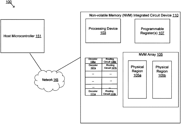
1. A non-volatile memory (NVM) integrated circuit device comprising:
a processing device;
an NVM array of memory cells partitioned into a first physical region and a second physical region;
a plurality of routing circuits;
a first decoder associated with a first routing circuit;
a second decoder associated with a second routing circuit;
a first programmable register coupled to the plurality of routing circuits, wherein the first programmable register is to store a first multi-bit value, the first multi-bit value programmed by the processing device to configure a first address range associated with the first decoder; and
a second programmable register coupled to the plurality of routing circuits, wherein the second programmable register is to store a second multi-bit value, the second multi-bit value programmed by the processing device to configure a second address range associated with the second decoder.
|