| CPC G06F 30/392 (2020.01) [G06F 30/27 (2020.01); G06F 2119/18 (2020.01)] | 20 Claims |

|
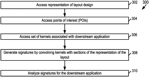
1. A computer-implemented method for analyzing a plurality of points of interest (POIs) in a semiconductor layout design for a downstream application, the method comprising:
accessing one or more kernels based on the downstream application, the one or more kernels when convolved with a representation of the semiconductor layout design extracting at least one feature associated with the plurality of POIs, the extracted at least one feature for use by the downstream application;
for a respective POI of the plurality of POIs, convolving the one or more kernels with the representation of the semiconductor layout design in order to generate a signature for the respective POI, wherein the one or more kernels comprise a set of mutually exclusive rings centered about the respective POI in order to generate the signature, the signature comprising a numerical representation indicative of the extracted at least one feature associated with the respective POI; and
analyzing, based on the downstream application, the signature for the extracted at least one feature associated with the respective POI.
|