| CPC G06F 3/0412 (2013.01) [G06F 3/04184 (2019.05); G09G 3/20 (2013.01); G09G 5/008 (2013.01); G09G 2330/021 (2013.01); G09G 2340/0435 (2013.01)] | 13 Claims |

|
1. A display driving device comprising:
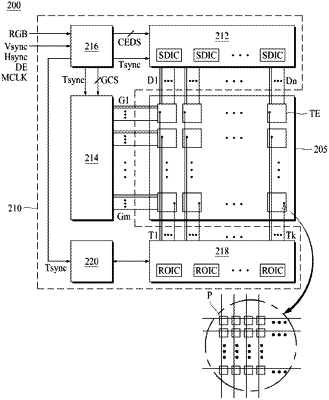
a source driver IC (integrated circuit) configured to operate in a first low power mode in which an analog data processing circuit is deactivated, or operate in a second low power mode in which both of the analog data processing circuit and a digital data processing circuit are deactivated, during a touch sensing period of a first frame;
a readout IC configured to supply touch sensor driving signals to touch sensors during the touch sensing period, and receive touch sensing data from the touch sensors according to the touch sensor driving signals; and
a timing controller configured to generate, during a display period of the first frame, a clock embedded data signaling (CEDS) packet including clock training data, control data, and image data, and transmit the CEDS packet to the source driver IC,
wherein, when the source driver IC operates in the first low power mode or the second low power mode during the touch sensing period, the timing controller sets a first voltage (VCEDN) and a second voltage (VCEDP) for generating the clock training data to the same level, control the source driver IC to be a high-impedance (Hi-Z) state or control the clock training data to be maintained at a predetermined level to prevent the clock training data from being transmitted.
|