US 12,032,508 B2
Interface clock management
Yuanlong Wang, San Jose, CA (US)
Assigned to Rambus Inc., San Jose, CA (US)
Filed by Rambus Inc., San Jose, CA (US)
Filed on May 8, 2023, as Appl. No. 18/144,349.
Application 18/144,349 is a continuation of application No. 17/559,975, filed on Dec. 22, 2021, granted, now 11,681,648.
Application 17/559,975 is a continuation of application No. 16/734,839, filed on Jan. 6, 2020, granted, now 11,238,003, issued on Feb. 1, 2022.
Application 16/734,839 is a continuation of application No. 15/794,148, filed on Oct. 26, 2017, granted, now 10,558,608, issued on Feb. 11, 2020.
Application 15/794,148 is a continuation of application No. 13/503,702, granted, now 9,824,056, issued on Nov. 21, 2017, previously published as PCT/US2010/054762, filed on Oct. 29, 2010.
Claims priority of provisional application 61/258,441, filed on Nov. 5, 2009.
Prior Publication US 2023/0350835 A1, Nov. 2, 2023
This patent is subject to a terminal disclaimer.
Int. Cl. G06F 13/42 (2006.01); G06F 1/3206 (2019.01); G06F 1/3234 (2019.01); G06F 1/3237 (2019.01)
CPC G06F 13/4243 (2013.01) [G06F 1/3206 (2013.01); G06F 1/3237 (2013.01); G06F 1/3275 (2013.01); Y02B 70/10 (2013.01); Y02D 10/00 (2018.01); Y02D 30/50 (2020.08)] 20 Claims
OG exemplary drawing
 
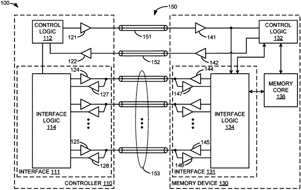
1. A controller, comprising:
an interface to transmit, to at least a first memory device and a second memory device, a first command that indicates a read of a status register;
a first receiver circuit to serially receive information from the status register; and
a second receiver to receive a resume signal collectively from the first memory device and the second memory device that indicates whether the first memory device and the second memory device are collectively ready to receive a clock signal that synchronizes a transmission of the information from the status register.