| CPC G02F 1/31 (2013.01) [G02F 2201/02 (2013.01); G02F 2202/20 (2013.01); G02F 2203/07 (2013.01)] | 17 Claims |
|
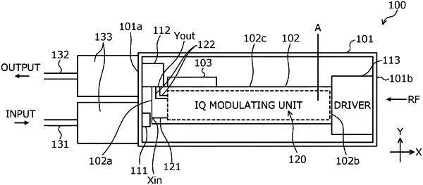
1. An optical modulator in which an optical signal is input and output from one side of a package, the optical modulator comprising:
in the package,
a chip that optically modulates an optical signal and in which an input waveguide and an output waveguide of the optical signal are led to mutually different destinations;
an input optical system coupled to the input waveguide of the chip; and
an output optical system coupled to the output waveguide of the chip,
wherein
the input waveguide is led from one end of the chip facing the one side of the package, and the output waveguide is led to an other end of the chip facing a side orthogonal to the one end of the chip in a plan view,
the input optical system is provided between the one side of the package and the one end of the chip such that the optical signal input from the one side of the package is input to the input waveguide through the input optical system, and
the output optical system is disposed along the other end of the chip such that the optical signal output from the chip is output from the one side of the package through the output optical system.
|