US 12,032,266 B2
Phase modulator and phase modulator array including the same
Junghyun Park, Seoul (KR); Yifei Wang, Stanford, CA (US); and Mark L. Brongersma, Stanford, CA (US)
Assigned to SAMSUNG ELECTRONICS CO., LTD., Suwon-si (KR); and The Board of Trustees of the Leland Stanford Junior University, Stanford, CA (US)
Filed by SAMSUNG ELECTRONICS CO., LTD., Suwon-si (KR); and The Board of Trustees of the Leland Stanford Junior University, Stanford, CA (US)
Filed on Jul. 9, 2021, as Appl. No. 17/371,821.
Claims priority of provisional application 63/049,903, filed on Jul. 9, 2020.
Claims priority of application No. 10-2021-0037549 (KR), filed on Mar. 23, 2021; and application No. 10-2021-0061637 (KR), filed on May 12, 2021.
Prior Publication US 2022/0013905 A1, Jan. 13, 2022
Int. Cl. G02F 1/01 (2006.01); G02F 1/29 (2006.01); H01Q 3/36 (2006.01); H01Q 3/46 (2006.01); H04B 7/06 (2006.01); H04B 10/548 (2013.01)
CPC G02F 1/292 (2013.01) [G02F 1/0147 (2013.01); H01Q 3/36 (2013.01); H01Q 3/46 (2013.01); H04B 7/0617 (2013.01); H04B 10/548 (2013.01); G02F 2203/10 (2013.01); G02F 2203/50 (2013.01)] 20 Claims
OG exemplary drawing
 
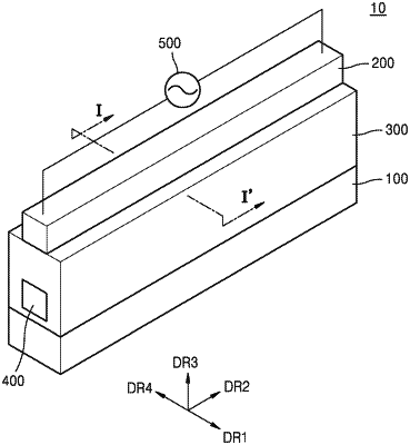
1. A phase modulator comprising:
an antenna pattern;
a lower reflective layer spaced apart from the antenna pattern in a vertical direction;
a spacer provided between the antenna pattern and the lower reflective layer, wherein the spacer comprises a first material; and
a phase shift pattern included in the spacer, the phase shift pattern comprising a phase shift material that is different from the first material,
wherein the spacer is provided on an upper surface, a lower surface and a first and second side of the phase shift pattern.