| CPC G02F 1/2257 (2013.01) [G02F 1/025 (2013.01); G02F 1/035 (2013.01); G02F 2202/103 (2013.01)] | 20 Claims |

|
1. A method comprising:
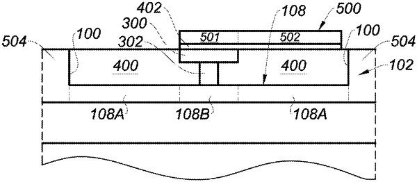
etching a cavity in a first silicon layer that overlies an insulating layer, the cavity having sidewalls and a floor;
epitaxially growing a germanium or silicon-germanium layer in the cavity, the germanium or silicon-germanium layer being grown from the floor of the cavity;
epitaxially growing a second silicon layer in the cavity, the second silicon layer being grown from the germanium or silicon-germanium layer to fill the cavity;
etching the second silicon layer and the germanium or silicon-germanium layer to the floor of the cavity to define a first strip in the second silicon layer and a second strip in the germanium or silicon-germanium layer, the first strip on the second strip and having the same width as the second strip;
selectively etching a portion of the second strip to decrease the width of the second strip so that the width of the first strip is greater than the width of the second strip;
etching a portion of the first silicon layer to expose a portion of the insulating layer between one edge of the first strip and one of the sidewalls;
filling cavity portions arranged on either side of the first and second strips with an insulator;
depositing an upper insulating layer over the first and second strips; and
bonding a layer of III-V material to the upper insulating layer.
|