| CPC G02F 1/13458 (2013.01) [G02F 1/134336 (2013.01); G02F 1/136286 (2013.01); G02F 1/1368 (2013.01); H01L 27/124 (2013.01)] | 15 Claims |
|
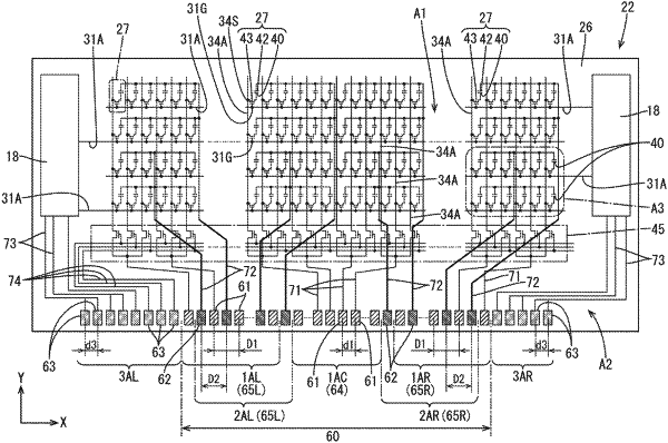
1. An active matrix substrate comprising:
a substrate;
pixel electrodes disposed on the substrate and arrayed in a matrix along a row direction and a column direction;
switching elements arranged in the row direction and the column direction on the substrate and connected to the pixel electrodes, respectively;
common electrodes arranged in the row direction and the column direction on the substrate;
a group of terminals disposed in an end section of the substrate with respect to the column direction and including a group of wire terminals and a group of common wire terminals, the group of wire terminals including two end wire terminals disposed at two ends of the group of wire terminals, the two end wire terminals including a first end wire terminal and a second end wire terminal;
a group of connection wires arranged in the row direction on the substrate corresponding to the wire terminals, respectively, and electrically connecting the wire terminals to the switching elements, the connection wires including first end portions and second end portions, respectively, the first end portions extending from the wire terminals, respectively, and the second end portions being opposite end portions opposite the first end portions,
the group of connection wires further including two end connection wires including a first end connection wire that extends from the first end wire terminal and a second end connection wire that extends from the second end wire terminal,
the first end wire terminal being away from the second end wire terminal with a first distance,
the second end portion of the first end connection wire being away from the second end portion of the second end connection wire with a second distance, and the first distance being smaller than the second distance; and
common wires arranged in the row direction on the substrate and electrically connecting the common wire terminals to the common electrodes, respectively, the common wires including third end portions that extend from the common wire terminals and fourth end portions that extend from the common electrodes, respectively, wherein
the common wire terminals include a first set and a second set, the first set including two common wire terminals that are adjacent to each other at a first set interval and the second set including other common wire terminals that are adjacent to each other at a second set interval, the second set interval is smaller than the first set interval,
one of the other common wire terminals included in the second set is connected to a common wire located at an outermost side of the common wires, and
a part of at least one of the connection wires is disposed between the third end portions of two common wires connected to the common wire terminals of the second set.
|