| CPC G02F 1/0147 (2013.01) [B29D 11/00932 (2013.01); G02F 1/212 (2021.01); G02F 1/2257 (2013.01)] | 8 Claims |

|
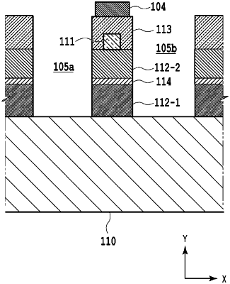
1. An optical signal processing device formed as a planar optical circuit comprising:
an optical waveguide formed on a silicon substrate, the optical waveguide comprising:
a phase modulation element that employs a thermo-optical effect;
a first silica thin film that is provided between a core of the optical waveguide and the silicon substrate;
a second silica thin film that is provided between the core of the optical waveguide and the silicon substrate;
a silicon laver that extends an entire width of an interface between the first silica thin film and the second silica thin film;
a first insulating groove; and
a second insulating groove,
wherein at least one of the first and second silica thin films was formed by thermal oxidation,
wherein the core of the optical waveguide is stacked on top the first silica thin film, the first silica thin film is stacked on top the silicon layer, the silicon layer is stacked on top of the second silica thin film, and the second silica thin film is stacked on top of the silicon substrate,
wherein a first width of the first silica thin film, the silicon layer, and the second silica thin laver are the same,
wherein a second width of the first and second insulating grooves is the same, and
wherein the second width of the first and second insulating grooves is larger than the first width of the first silica thin film, the silicon layer, and the second silica thin layer.
|