| CPC G02B 5/3091 (2013.01) [G02B 3/0018 (2013.01); G02B 5/3016 (2013.01); G02B 5/3041 (2013.01)] | 7 Claims |

|
1. An optical element comprising:
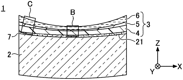
a three-dimensional structure having a curved surface; and
a retardation plate bent along the curved surface, wherein
the retardation plate includes a transparent substrate, an alignment layer formed over the transparent substrate, and a liquid crystal layer formed over the alignment layer,
the retardation plate has a slow axis and a fast axis,
the alignment layer has a plurality of grooves parallel to each other on a surface in contact with the liquid crystal layer when viewed from a direction normal to the curved surface of the three-dimensional structure at a center of gravity of the curved surface,
a depth of a groove at a position where a thickness of the retardation plate is thinnest is deeper than a depth of a groove at a position where the thickness of the retardation plate is thickest, and
a glass-transition temperature, Tgne, in a slow axis direction of the retardation plate is higher than a glass-transition temperature, Tgno, in a fast axis direction of the retardation plate.
|