| CPC G02B 5/28 (2013.01) [G02B 1/045 (2013.01); G02B 6/0043 (2013.01); G02B 6/0065 (2013.01); G02B 2207/101 (2013.01)] | 20 Claims |

|
1. A color filter substrate, comprising:
a base; and
a color filter structure on a side of the base,
wherein the color filter substrate comprises a plurality of pixel regions, and each of the plurality of pixel regions comprises a plurality of sub-pixel regions;
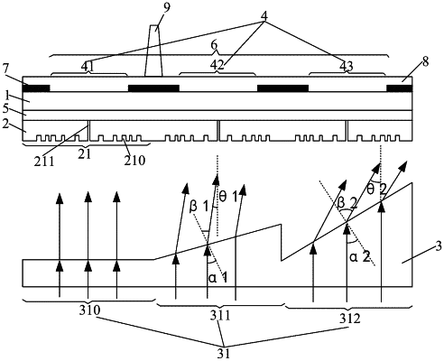
the color filter structure comprises a nanostructure layer and a light guide structure layer, the light guide structure layer is on a side of the nano structure layer distal to the base, the light guide structure layer comprises a plurality of light guide structures, each of the plurality of light guide structures is in a corresponding one of the plurality of pixel regions, each of the plurality of light guide structures comprises a plurality of light guide sub-portions, each of the plurality of light guide sub-portions is in a corresponding one of the plurality of sub-pixel regions of the pixel region in which the light guide sub-portion is located, the nanostructure layer comprises a plurality of non-periodic nanostructures, each of the plurality of sub-pixel regions corresponds to at least one of the non-periodic nanostructures, and each of the plurality of non-periodic nanostructures is in a corresponding one of the plurality of sub-pixel regions; and
each of the plurality of light guide sub-portions in a same pixel region is configured such that light incident respectively on the plurality of light guide sub-portions in the same pixel region exits at different angles and enters into the at least one non-periodic nanostructure in the sub-pixel region in which the light guide sub-portion is located, and each non-periodic nanostructure is configured to enable coupling and interference of light incident thereon such that light exiting from the sub-pixel region in which the non-periodic nanostructure is located has a predetermined color.
|