| CPC G01R 31/318552 (2013.01) [G01R 31/318541 (2013.01)] | 19 Claims |

|
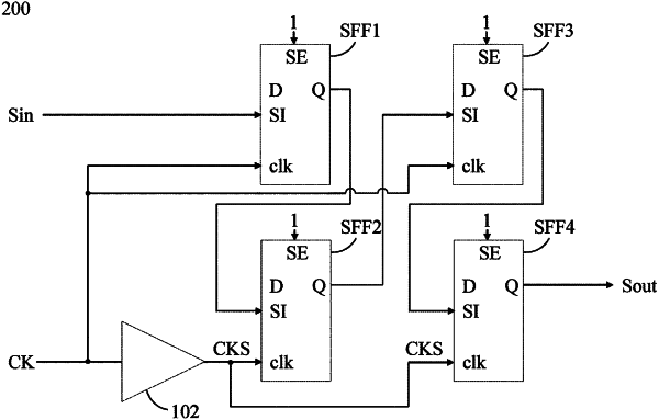
1. A calibration data generation circuit, comprising:
a first delay unit, having first delay amount;
a first scan path, comprising:
a first scan flip-flop, comprising:
a scan data input terminal;
a clock input terminal, configured to receive a clock signal; and
an output terminal; and
a second scan flip-flop, comprising:
a scan data input terminal, coupled to the output terminal of the first scan flip-flop;
a clock input terminal, configured to receive a first delayed clock signal formed by the clock signal passing through the first delay unit; and
an output terminal; and
a second scan path, comprising:
a third scan flip-flop, comprising:
a scan data input terminal;
a clock input terminal, configured to receive the clock signal; and
an output terminal; and
a fourth scan flip-flop, comprising:
a scan data input terminal, coupled to the output terminal of the third scan flip-flop;
a clock input terminal, configured to receive the first delayed clock signal; and
an output terminal;
wherein when the calibration data generation circuit is configured to perform a first scan shift operation on the first scan path and a second scan shift operation on the second scan path, the first scan flip-flop and the second scan flip-flop are configured in a scan shift mode to obtain a first scan shift result for calibrating a default timing derate factor, and the third scan flip-flop and the fourth scan flip-flop are configured in the scan shift mode to obtain a second scan shift result for calibrating the default timing derate factor.
|