| CPC G01R 31/3177 (2013.01) [G01R 31/2834 (2013.01); G01R 31/3004 (2013.01); G01R 31/31727 (2013.01); G01R 31/31924 (2013.01); H03K 3/017 (2013.01); H03K 19/21 (2013.01); H03L 7/099 (2013.01); H01L 22/34 (2013.01); H01L 2924/00 (2013.01); H01L 2924/0002 (2013.01)] | 20 Claims |

|
1. A clock conversion device comprising:
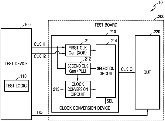
a first clock generator configured to receive a first input clock signal from test logic and generate a first clock signal of which a frequency is multiplied and a phase is locked;
a clock conversion circuit configured to receive the first clock signal and generate one or more second clock signals by converting at least one clock characteristic of the first clock signal; and
an output selector configured to output any one of the first clock signal and the one or more second clock signals as an output clock signal,
wherein the clock conversion device is configured to provide the output clock signal to a device under test (DUT).
|