| CPC G01R 31/2851 (2013.01) [G01R 31/2831 (2013.01); G01R 31/2834 (2013.01); G01R 31/2884 (2013.01); G01R 31/2886 (2013.01); H01L 22/34 (2013.01); H01L 2924/00 (2013.01); H01L 2924/0002 (2013.01)] | 23 Claims |

|
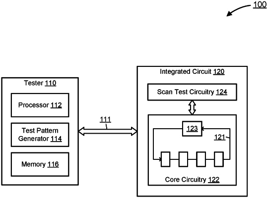
1. An integrated circuit device, comprising:
core circuitry;
a set of configuration registers; and
scan test circuitry configured to:
selectively allocate, according to a first scan configuration stored in the set of configuration registers, a first set of scan-in test pads to a corresponding first set of scan input channels of a first scan domain that includes a first set of core circuitry blocks in the core circuitry, and a first set of scan-out test pads to a corresponding first set of scan output channels of the first scan domain;
perform scan testing of the first scan domain by receiving a first test pattern on the first set of scan-in test pads, transmitting the first test pattern to the first scan domain via the first set of scan input channels, receiving a first test response on the first set of scan output channels, and transmitting the first test response to the first set of scan-out test pads;
selectively allocate, according to a second scan configuration stored in the set of configuration registers, a second set of scan-in test pads to a corresponding second set of scan input channels of a second scan domain that includes a second set of core circuitry blocks in the core circuitry, and a second set of scan-out test pads to a corresponding second set of scan output channels of the second scan domain; and
perform scan testing of the second scan domain by receiving a second test pattern on the second set of scan-in test pads, transmitting the second test pattern to the second scan domain via the second set of scan input channels, receiving a second test response on the second set of scan output channels, and transmitting the second test response to the second set of scan-out test pads.
|