| CPC G01R 31/2608 (2013.01) [H01L 27/0722 (2013.01); H01L 29/1095 (2013.01); H01L 29/735 (2013.01); H01L 29/7816 (2013.01)] | 20 Claims |
|
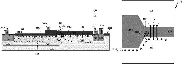
1. A semiconductor device configured with gate dielectric monitoring capability, the semiconductor device comprising:
a metal-oxide-semiconductor (MOS) transistor including a source, a drain, a gate, and a backgate region formed in a semiconductor substrate; and
a bipolar junction transistor (BJT) including a collector, a base, and an emitter formed in the semiconductor substrate, wherein the backgate region of the MOS transistor serves as the base of the BJT and is independently accessible for activating the BJT,
wherein the MOS transistor and the BJT are configured to be concurrently activated by biasing the backgate region independently from the source of the MOS transistor, such that the base of the BJT injects carriers of a first charge type into the backgate region of the MOS transistor, the first charge type being opposite charge type to channel current carriers.
|