| CPC G01N 33/56983 (2013.01) [C01B 32/198 (2017.08); C01B 32/26 (2017.08); C23C 16/0236 (2013.01); C23C 16/271 (2013.01); C23C 16/274 (2013.01); C23C 16/279 (2013.01); C23C 16/513 (2013.01); G01N 27/4145 (2013.01); G01N 33/551 (2013.01); H01L 29/66969 (2013.01); B82Y 5/00 (2013.01); B82Y 30/00 (2013.01); B82Y 35/00 (2013.01); B82Y 40/00 (2013.01); C01B 2204/22 (2013.01); C01B 2204/32 (2013.01); C01P 2002/60 (2013.01); C01P 2004/16 (2013.01); C01P 2004/64 (2013.01); G01N 2333/165 (2013.01)] | 20 Claims |

|
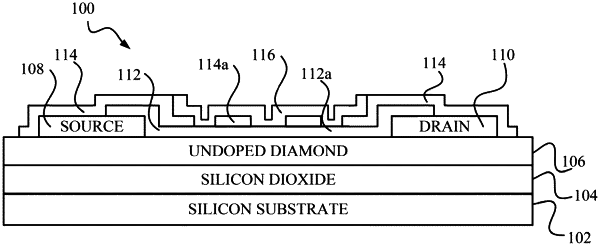
1. A transistor pathogen detector, comprising:
A substrate layer,
a silicon dioxide layer on the substrate layer,
a nanocrystalline diamond layer on the silicon dioxide layer,
a graphene oxide layer on the nanocrystalline diamond layer,
fluorinated graphene oxide portions; and
a linker layer, the linker layer including a plurality of pathogen receptors, wherein the transistor pathogen detector functions as a biosensor field effect transistor.
|