| CPC G01N 29/022 (2013.01) [G01N 29/2462 (2013.01); G01N 2291/0423 (2013.01); G01N 2291/0426 (2013.01)] | 15 Claims |
|
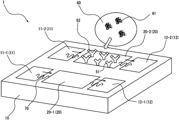
1. A sensor device comprising:
a substrate having a substrate surface;
a first IDT electrode and a second IDT electrode that are positioned on the substrate surface; and
a waveguide that is positioned on the substrate surface and between the first IDT electrode and the second IDT electrode,
wherein the first IDT electrode and the second IDT electrode includes a reference electrode and a signal electrode each including a plurality of electrode fingers, the plurality of electrode fingers being arranged in a juxtaposed manner in one direction,
wherein a distance between the at least one of the first IDT electrode and the second IDT electrode and the waveguide is shorter than an interval between the reference electrode and the signal electrode in the one direction, and
wherein the at least one of the first IDT electrode and the second IDT electrode is positioned away from the waveguide.
|