| CPC G01N 27/02 (2013.01) [G01N 33/0027 (2013.01)] | 15 Claims |
|
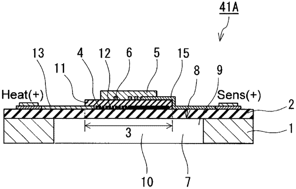
1. A gas sensor comprising:
a substrate;
a support layer;
a base layer;
a heater layer disposed on or above the base layer;
a gas sensing layer disposed on or above one of the heater layer and the base layer, the gas sensing layer having an electrical impedance that is gas concentration dependent; and
a detection electrode electrically connected to the gas sensing layer, the detection electrode detecting the impedance of the gas sensing layer,
wherein the substrate has a cavity,
wherein the substrate has an opening formed by the cavity in plan view,
wherein the support layer is disposed on the substrate so as to cover at least an entire periphery of the opening,
wherein the base layer is supported by the support layer above the cavity so as to be separated from the substrate, and
wherein the support layer has a first phononic crystal structure in a portion in contact with the cavity, and the first phononic crystal structure is structured by a plurality of regularly arranged through-holes.
|