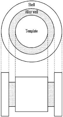
| CPC C09K 11/565 (2013.01) [C08J 5/18 (2013.01); C09K 11/06 (2013.01); C09K 11/54 (2013.01); C09K 11/62 (2013.01); C09K 11/70 (2013.01); H10K 50/115 (2023.02); B82Y 20/00 (2013.01); B82Y 30/00 (2013.01); B82Y 40/00 (2013.01); C08J 2300/12 (2013.01)] | 30 Claims |

|
1. A quantum dot comprising
a template comprising a first semiconductor nanocrystal,
a quantum well layer disposed on the template, and
a shell disposed on the quantum well layer, the shell comprising a second semiconductor nanocrystal,
wherein the quantum dot does not comprise cadmium,
wherein the first semiconductor nanocrystal comprises a first zinc chalcogenide,
wherein the second semiconductor nanocrystal comprises a second zinc chalcogenide,
wherein the quantum well layer comprises an alloy semiconductor nanocrystal comprising indium, phosphorus, zinc, and a chalcogen element, and
wherein a bandgap energy of the alloy semiconductor nanocrystal is less than a bandgap energy of the first semiconductor nanocrystal and less than a bandgap energy of the second semiconductor nanocrystal.
|