| CPC B81C 1/00238 (2013.01) [B81B 7/0006 (2013.01); G01L 9/0041 (2013.01); B81B 2201/0264 (2013.01); B81B 2207/012 (2013.01); B81B 2207/07 (2013.01); B81C 2203/035 (2013.01); B81C 2203/0792 (2013.01)] | 16 Claims |
|
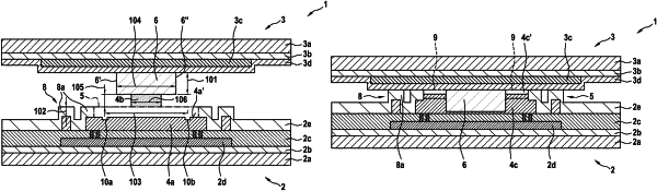
1. A method for producing a wafer connection between a first wafer and a second wafer, the method comprising:
providing a first material and a second material for forming a eutectic alloy;
providing the first wafer having a receiving structure for a die structure;
filling the receiving structure with the first material;
providing the second wafer having a die structure, the second material being situated on the die structure;
providing a stop structure on the first wafer and/or the second wafer, so that when the first wafer and the second wafer are joined, a defined stop is provided;
heating at least the first material and the second material at least to a eutectic temperature of the eutectic alloy; and
joining the first and second wafer so that the die structure is at least partly introduced into the receiving structure;
wherein the stop structure, the receiving structure, the die structure, and a quantity of the first material and the second material are dimensioned such that after the joining of the first wafer and the second wafer, the eutectic alloy of the first material and the second material remains within the receiving structure, and the die structure is at least partly surrounded by the eutectic alloy.
|
|
15. A micro-electro-mechanical system (MEMS) sensor, comprising:
a die structure;
a first wafer having a receiving structure, which is in the form of a trough and which receives the die structure;
a second wafer;
a stop structure situated on the first wafer and/or the second wafer to provide a defined distance between the first wafer and the second wafer, wherein the die structure provides a mechanical connection between the first wafer and the second wafer; and
a eutectic alloy material in the receiving structure, wherein the eutectic alloy material is formed from a first material and a second material, and wherein the die structure is in the receiving structure and is at least partly surrounded by the eutectic alloy material.
|