| CPC B22F 7/064 (2013.01) [B22F 1/00 (2013.01); B22F 1/107 (2022.01); H01L 24/29 (2013.01); H01L 24/32 (2013.01); H01L 24/83 (2013.01); H01L 2224/29147 (2013.01); H01L 2224/32058 (2013.01); H01L 2224/32245 (2013.01); H01L 2224/83192 (2013.01); H01L 2224/83203 (2013.01); H01L 2224/8384 (2013.01)] | 9 Claims |

|
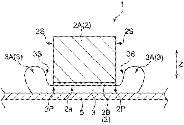
1. A bonded body comprising:
a bonding layer containing Cu; and
a semiconductor element bonded to the bonding layer,
wherein the bonding layer includes an extending portion laterally extending from a peripheral edge of the semiconductor element,
in a cross-sectional view in a thickness direction, the extending portion rises from a peripheral edge of a bottom of the semiconductor element or from a vicinity of the peripheral edge of the bottom of the semiconductor element, and includes a side wall substantially spaced apart from a side of the semiconductor element,
a side of the semiconductor element contacts the extending portion at a contact portion,
a length of the contact portion in the thickness direction in the cross-sectional view is 20 μm or less, and
a length of the contact portion in a planar direction in a plan view is 20 μm or less.
|