| CPC H10K 71/00 (2023.02) [H10K 50/805 (2023.02); H10K 50/824 (2023.02); H10K 59/122 (2023.02); H10K 59/173 (2023.02); H10K 59/35 (2023.02); H10K 71/166 (2023.02); H10K 71/221 (2023.02); H10K 71/621 (2023.02); H10K 59/1201 (2023.02)] | 20 Claims |
|
1. An organic light-emitting display apparatus comprising:
a substrate;
a plurality of first thin film transistors and a plurality of second thin film transistors arranged on the substrate;
a plurality of first anodes on the substrate, the plurality of first anodes being spaced apart from each other along a first direction, and each of the plurality of first anodes being electrically connected to a corresponding one of the plurality of first thin film transistors;
a plurality of second anodes on the substrate, the plurality of second anodes being spaced apart from the plurality of first anodes in a second direction that intersects with the first direction, the plurality of second anodes being spaced apart from each other along the first direction, and each of the plurality of second anodes being electrically connected to a corresponding one of the plurality of second thin film transistors;
a pixel defining layer surrounding edges of both the plurality of first anodes and the plurality of second anodes;
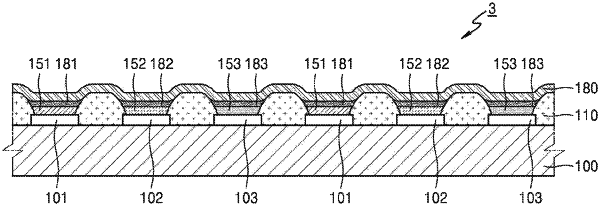
a first organic functional layer continuously arranged in the first direction on the plurality of first anodes and on the pixel defining layer between the plurality of first anodes, the first organic functional layer comprising a first emission layer;
a second organic functional layer continuously arranged in the first direction on the plurality of second anodes and on the pixel defining layer between the plurality of second anodes, the second organic functional layer comprising a second emission layer;
a first auxiliary cathode on the first organic functional layer; and
a second auxiliary cathode on the second organic functional layer,
wherein the first auxiliary cathode is spaced apart from the second auxiliary cathode in the second direction.
|