| CPC H10K 71/00 (2023.02) [H10K 59/12 (2023.02); H10K 59/1201 (2023.02)] | 20 Claims |
|
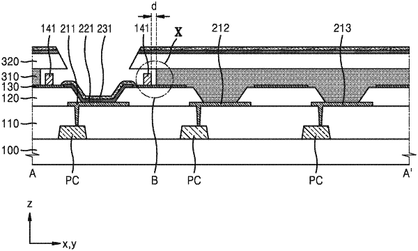
1. A method of manufacturing a display apparatus, the method comprising:
forming a first pixel electrode for emission of a first color on a substrate;
forming an insulating layer, the insulating layer covering edges of the first pixel electrode, and defining a first opening exposing a center portion of the first pixel electrode;
forming a first dam portion on the insulating layer around the first opening;
forming a first lift-off layer on the insulating layer around an outside of the first dam portion and defining an opening exposing the first pixel electrode;
forming a first mask layer on the first lift-off layer, the first mask layer defining a first open portion corresponding to the first opening;
forming a first intermediate layer on the first pixel electrode through the first open portion;
forming a first opposite electrode on the first intermediate layer through the first open portion;
forming a first insulating protective layer on the first opposite electrode through the first open portion; and
removing the first mask layer, the first lift-off layer, and the first dam portion.
|