| CPC H10K 59/40 (2023.02) [H10K 50/84 (2023.02); H10K 59/131 (2023.02); H10K 71/00 (2023.02); H10K 2102/00 (2023.02)] | 16 Claims |
|
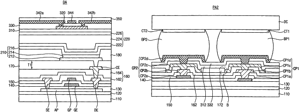
13. A display device comprising:
a pixel array at a display area;
a connection pad at a bonding area, the connection pad comprising a lower conductive layer, an intermediate conductive layer on the lower conductive layer, and an upper conductive layer on the intermediate conductive layer;
a cladding layer covering at least a side surface of the intermediate conductive layer and comprising an organic material;
a passivation layer covering an upper surface of the cladding layer and comprising an inorganic material, a portion of the passivation layer being located under a portion of the upper conductive layer overlapping with the lower conductive layer; and
a driving circuit attached to the connection pad,
wherein the connection pad comprises a first connection pad and a second connection pad adjacent to the first connection pad, and the cladding layer is located between the first and second connection pads to cover at least side surfaces of the intermediate conductive layers of the first and second connection pads that face each other, while the passivation layer covering the upper surface of the cladding layer extends between the first and second connection pads at the bonding area and contacts an upper surface of the intermediate conductive layer.
|