| CPC H10K 59/126 (2023.02) [G06F 3/0412 (2013.01); G06V 40/1318 (2022.01); G09G 3/3233 (2013.01); G09G 3/3258 (2013.01); H01L 25/18 (2013.01); H10K 59/131 (2023.02); G06F 3/0443 (2019.05); G06F 3/0446 (2019.05); G09G 2310/0202 (2013.01); G09G 2360/14 (2013.01); H10K 59/353 (2023.02)] | 20 Claims |
|
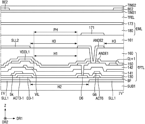
1. A display device comprising:
a substrate;
a first light blocking layer including a first hole and located on the substrate;
a buffer film on the first light blocking layer;
an active layer on the buffer film;
a first insulating film on the active layer;
a first gate layer on the first insulating film;
a second insulating film on the first gate layer;
a second gate layer on the second insulating film;
a third insulating film on the second gate layer;
a data metal layer on the third insulating film;
a first organic layer on the data metal layer;
a second light blocking layer including a second hole and located on the first organic layer;
a second organic layer on the second light blocking layer; and
a light emitting element on the second organic layer,
wherein a third hole is defined by the active layer, the first gate layer, the second gate layer, and the data metal layer.
|