| CPC H10K 59/122 (2023.02) [G03F 7/40 (2013.01); H10K 50/805 (2023.02); H10K 50/824 (2023.02); H10K 59/124 (2023.02); H10K 71/00 (2023.02); H10K 71/221 (2023.02); H10K 71/233 (2023.02); H10K 59/1201 (2023.02); H10K 59/35 (2023.02)] | 9 Claims |

|
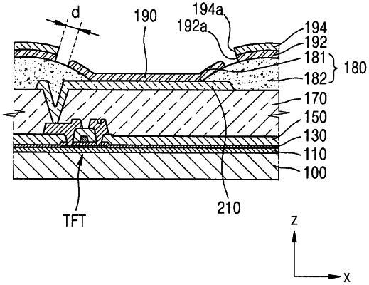
1. A method of manufacturing a display device, the method comprising:
forming a pixel electrode on a substrate;
forming a pixel-defining layer having a first opening exposing a central portion of the pixel electrode and a barrier portion defining the first opening;
forming a first photosensitive layer on the pixel electrode so as to cover the first opening;
forming an auxiliary electrode on the barrier portion, wherein the auxiliary electrode has a second opening exposing the first photosensitive layer;
forming a second photosensitive layer on the auxiliary electrode, wherein the second photosensitive layer has a third opening exposing the first photosensitive layer; and
removing the first photosensitive layer and the second photosensitive layer.
|