| CPC H10K 50/858 (2023.02) [H10K 59/126 (2023.02); H10K 59/65 (2023.02); H10K 2102/351 (2023.02)] | 20 Claims |
|
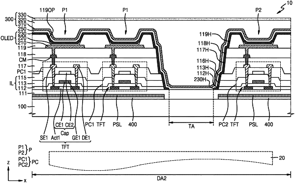
1. A display panel having a transmittance area and comprising:
a substrate;
first pixel circuits and second pixel circuits on the substrate and spaced apart from one another with the transmittance area therebetween, and each comprising a thin film transistor and a storage capacitor;
first display elements electrically respectively coupled to the first pixel circuits;
second display elements electrically respectively coupled to the second pixel circuits; and
a first phase shift layer between the substrate and the first pixel circuits and between the substrate and the second pixel circuits and having a first light transmittance,
wherein the first phase shift layer does not extend through the transmittance area.
|