| CPC H10K 50/8426 (2023.02) [G06F 3/0412 (2013.01); H10K 59/12 (2023.02); H10K 59/40 (2023.02); H10K 71/00 (2023.02); G06F 2203/04103 (2013.01); H10K 59/1201 (2023.02); H10K 2102/351 (2023.02)] | 36 Claims |
|
1. A display device comprising:
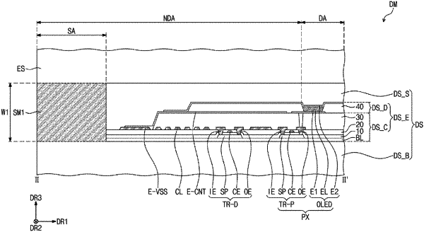
a display module on which a display area and at non-display area configured to surround the display area are defined on a plane,
wherein the display module comprises:
a display substrate comprising a plurality of pixels disposed on the display area and comprising a glass material; and
an encapsulation substrate disposed to face the display substrate and comprising a glass material,
wherein the non-display area comprises a sealing area on which the display substrate and the encapsulation substrate are bonded to each other, and
a portion of the sealing area has a width of about 50 um to about 110 um.
|