| CPC H10K 50/19 (2023.02) [H10K 50/13 (2023.02); H10K 59/123 (2023.02); H10K 59/38 (2023.02); H10K 50/15 (2023.02); H10K 50/16 (2023.02); H10K 50/17 (2023.02); H10K 50/171 (2023.02); H10K 71/00 (2023.02); H10K 85/30 (2023.02); H10K 85/322 (2023.02); H10K 85/615 (2023.02); H10K 85/626 (2023.02); H10K 85/633 (2023.02); H10K 85/636 (2023.02); H10K 85/654 (2023.02); H10K 85/6572 (2023.02); H10K 85/6574 (2023.02); H10K 2101/30 (2023.02); H10K 2102/331 (2023.02); H10K 2102/351 (2023.02)] | 17 Claims |
|
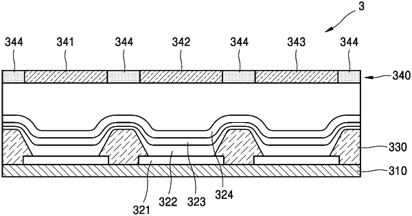
1. A light-emitting device comprising:
a first electrode;
a second electrode facing the first electrode;
light-emitting units in the number of n between the first electrode and the second electrode; and
a charge-generation unit(s) in the number of n−1 between the adjacent light-emitting units,
wherein n is a natural number of 2 or more,
the light-emitting units each comprise an emission layer,
at least one of the charge-generation unit(s) comprises an n-type charge-generation layer, a p-type charge-generation layer, and an interlayer between the n-type charge-generation layer and the p-type charge-generation layer,
the p-type charge-generation layer comprises a first material and a second material,
the first material comprises a hole-transporting organic compound, an inorganic insulation compound, or any combination thereof,
the second material comprises at least one inorganic semiconductor compound, and
the interlayer consists of a third material, the third material being at least one selected from a quinone derivative, 1,4,5,8,9,11-hexaazatriphenylene-hexacarbonitrile (HAT-CN), and a compound represented by Formula 221:
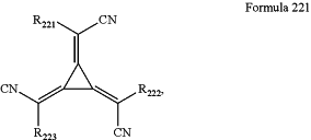 wherein in Formula 221,
each of R221 to R223 is independently selected from a substituted or unsubstituted C3-C10 cycloalkyl group, a substituted or unsubstituted C1-C10 heterocycloalkyl group, a substituted or unsubstituted C3-C10 cycloalkenyl group, a substituted or unsubstituted C1-C10 heterocycloalkenyl group, a substituted or unsubstituted C6-C60 aryl group, a substituted or unsubstituted C1-C60 heteroaryl group, a substituted or unsubstituted monovalent non-aromatic condensed polycyclic group, and a substituted or unsubstituted monovalent non-aromatic condensed heteropolycyclic group, and
wherein at least one selected from R221 to R223 has at least one substituent selected from a cyano group, —F, —Cl, —Br, —I, a C1-C20 alkyl group substituted with —F, a C1-C20 alkyl group substituted with —Cl, a C1-C20 alkyl group substituted with —Br, and a C1-C20 alkyl group substituted with —I.
|