| CPC H10K 50/115 (2023.02) [H10K 50/11 (2023.02); H10K 50/15 (2023.02); H10K 50/16 (2023.02); H10K 50/171 (2023.02); H10K 2101/40 (2023.02)] | 10 Claims |
|
1. A light-emitting device, comprising:
a substrate;
an anode;
a cathode; and
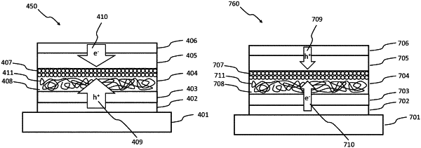
an emissive layer between the anode and the cathode, the emissive layer comprising quantum dots having ligands, a cross-linked matrix comprising a cross-linkable charge transport material other than the ligands, and another charge transport material,
wherein:
the quantum dots are dispersed in the cross-linked matrix,
the another charge transport material alters mobility of charge carriers of the emissive layer,
the cross-linkable charge transport material is a cross-linkable hole transporting material,
the another charge transport material is an efficient hole transporting material that improves hole mobility more than the cross-linkable charge transport material, and
in the emissive layer, the quantum dots and the another charge transport material are layer-separated from each other such that the quantum dots are close to the cathode and the another charge transport material is close to the anode.
|