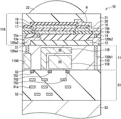
| CPC H10K 39/32 (2023.02) [H01L 27/146 (2013.01); H01L 31/10 (2013.01); H10K 19/20 (2023.02); H10K 30/353 (2023.02); H10K 71/164 (2023.02); H10K 85/631 (2023.02); H01L 27/14647 (2013.01); H01L 27/14689 (2013.01); H10K 30/30 (2023.02); H10K 85/211 (2023.02); H10K 85/215 (2023.02); H10K 85/322 (2023.02); H10K 85/622 (2023.02); H10K 85/626 (2023.02); H10K 85/633 (2023.02); H10K 85/6572 (2023.02); H10K 85/6576 (2023.02); Y02E 10/549 (2013.01)] | 34 Claims |

|
1. A photoelectric conversion element, comprising:
a first electrode and a second electrode facing each other; and
a photoelectric conversion layer provided between the first electrode and the second electrode, and including a first organic semiconductor material, a second organic semiconductor material, and a third organic semiconductor material that have mother skeletons different from one another,
wherein the first organic semiconductor material is one of fullerenes and fullerene derivatives,
wherein the second organic semiconductor material is formed as a single-layer film having a maximal light absorption wavelength in a visible light region in a range from 500 nm to 600 nm both inclusive, and
wherein the third organic semiconductor material is formed as a single-layer film having a higher hole mobility than a hole mobility of the single-layer film of the second organic semiconductor material.
|